- 您现在的位置:买卖IC网 > Sheet目录3896 > PIC16F505T-I/SL (Microchip Technology)IC MCU FLASH 1KX12 14SOIC
2009 Microchip Technology Inc.
DS41236E-page 25
PIC12F508/509/16F505
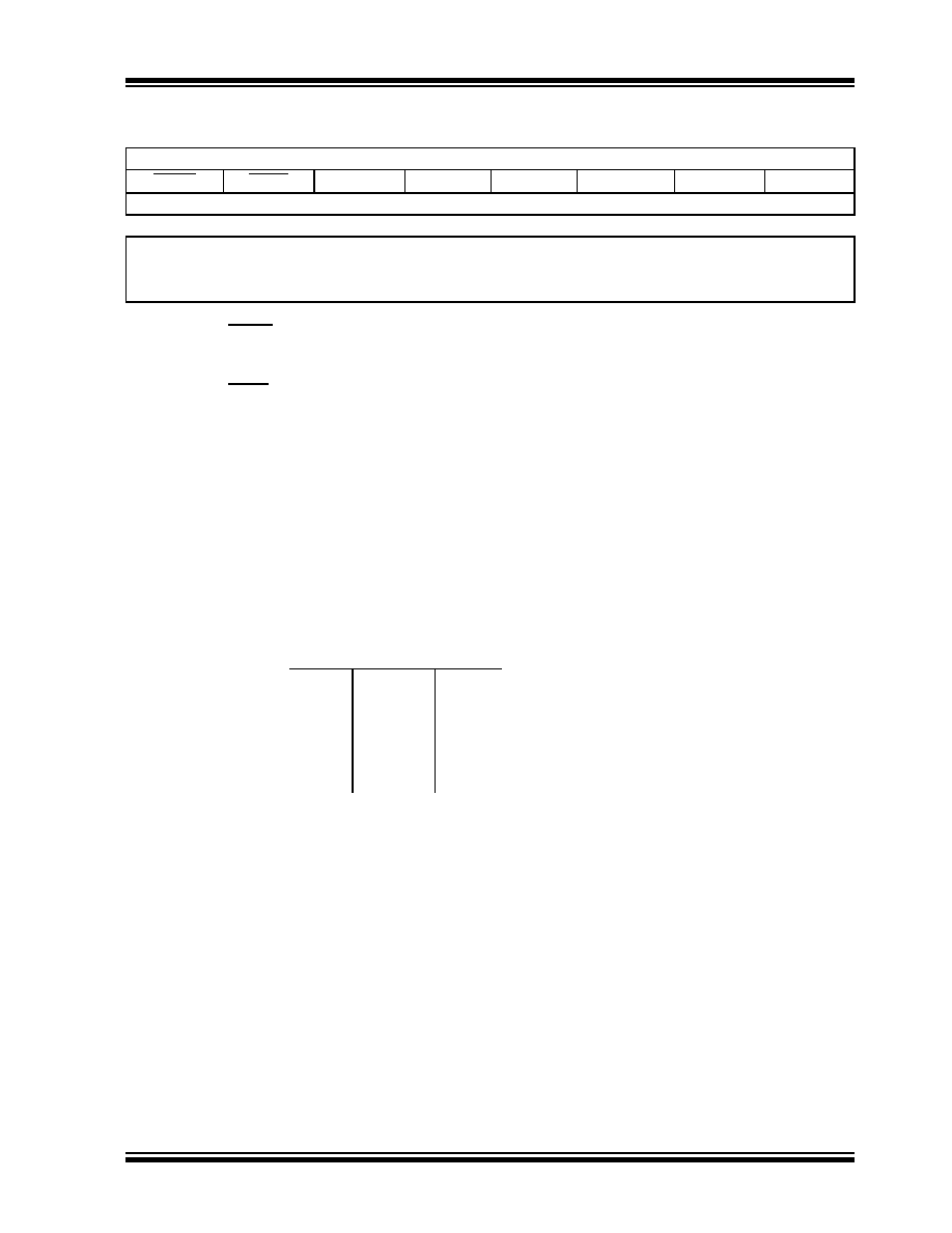
REGISTER 4-4:
OPTION REGISTER (PIC16F505)
W-1
RBWU
RBPU
T0CS
T0SE
PSA
PS2
PS1
PS0
bit 7
bit 0
Legend:
R = Readable bit
W = Writable bit
U = Unimplemented bit, read as ‘0’
-n = Value at POR
‘1’ = Bit is set
‘0’ = Bit is cleared
x = Bit is unknown
bit 7
RBWU: Enable Wake-up on Pin Change bit (RB0, RB1, RB3, RB4)
1
= Disabled
0
= Enabled
bit 6
RBPU: Enable Weak Pull-ups bit (RB0, RB1, RB3, RB4)
1
= Disabled
0
= Enabled
bit 5
T0CS: Timer0 clock Source Select bit
1
= Transition on T0CKI pin (overrides TRIS on the T0CKI pin)
0
= Transition on internal instruction cycle clock, FOSC/4
bit 4
T0SE: Timer0 Source Edge Select bit
1
= Increment on high-to-low transition on the T0CKI pin
0
= Increment on low-to-high transition on the T0CKI pin
bit 3
PSA: Prescaler Assignment bit
1
= Prescaler assigned to the WDT
0
= Prescaler assigned to Timer0
bit 2-0
PS<2:0>: Prescaler Rate Select bits
000
001
010
011
100
101
110
111
1 : 2
1 : 4
1 : 8
1 : 16
1 : 32
1 : 64
1 : 128
1 : 256
1 : 1
1 : 2
1 : 4
1 : 8
1 : 16
1 : 32
1 : 64
1 : 128
Bit Value
Timer0 Rate WDT Rate
发布紧急采购,3分钟左右您将得到回复。
相关PDF资料
PIC12F509T-I/SN
IC MCU FLASH 1KX12 8SOIC
PIC10F200T-E/OT
IC PIC MCU FLASH 256X12 SOT23-6
006200516230000
CONN FFC/FPC 16POS 1MM R/A SMD
006200516230000+
CONN FFC/FPC 16POS 1MM R/A SMD
40FMN-BMT-A-TF
CONN FMN HSNG 40POS SNGL NOR SMD
0781191309
CONN FFC/FPC 30POS .5MM VERT SMD
046214012010800+
CONN FPC VERTICAL 0.5 MM 12POS
006200514230000+
CONN FFC/FPC 14POS 1MM R/A SMD
相关代理商/技术参数
PIC16F505T-I/SL040
制造商:Microchip Technology Inc 功能描述:MCCPIC16F505T-I/SL040 14 PIN 1.5 KB F
PIC16F505T-I/ST
功能描述:8位微控制器 -MCU 2 KB 72 RAM 12 I/O RoHS:否 制造商:Silicon Labs 核心:8051 处理器系列:C8051F39x 数据总线宽度:8 bit 最大时钟频率:50 MHz 程序存储器大小:16 KB 数据 RAM 大小:1 KB 片上 ADC:Yes 工作电源电压:1.8 V to 3.6 V 工作温度范围:- 40 C to + 105 C 封装 / 箱体:QFN-20 安装风格:SMD/SMT
PIC16F506-E/MG
功能描述:8位微控制器 -MCU 1.5KB 67 RAM 12 I/O RoHS:否 制造商:Silicon Labs 核心:8051 处理器系列:C8051F39x 数据总线宽度:8 bit 最大时钟频率:50 MHz 程序存储器大小:16 KB 数据 RAM 大小:1 KB 片上 ADC:Yes 工作电源电压:1.8 V to 3.6 V 工作温度范围:- 40 C to + 105 C 封装 / 箱体:QFN-20 安装风格:SMD/SMT
PIC16F506-E/P
功能描述:8位微控制器 -MCU 1.5KB FL 67 RAM 12I/O Comp Ext Temp RoHS:否 制造商:Silicon Labs 核心:8051 处理器系列:C8051F39x 数据总线宽度:8 bit 最大时钟频率:50 MHz 程序存储器大小:16 KB 数据 RAM 大小:1 KB 片上 ADC:Yes 工作电源电压:1.8 V to 3.6 V 工作温度范围:- 40 C to + 105 C 封装 / 箱体:QFN-20 安装风格:SMD/SMT
PIC16F506-E/SL
功能描述:8位微控制器 -MCU 1.5KB Flsh 67RM 12IO Comp 8B ADC Ext Temp RoHS:否 制造商:Silicon Labs 核心:8051 处理器系列:C8051F39x 数据总线宽度:8 bit 最大时钟频率:50 MHz 程序存储器大小:16 KB 数据 RAM 大小:1 KB 片上 ADC:Yes 工作电源电压:1.8 V to 3.6 V 工作温度范围:- 40 C to + 105 C 封装 / 箱体:QFN-20 安装风格:SMD/SMT
PIC16F506-E/ST
功能描述:8位微控制器 -MCU 1.5 KB Flash 67RAM12 I/O 8bit ADC RoHS:否 制造商:Silicon Labs 核心:8051 处理器系列:C8051F39x 数据总线宽度:8 bit 最大时钟频率:50 MHz 程序存储器大小:16 KB 数据 RAM 大小:1 KB 片上 ADC:Yes 工作电源电压:1.8 V to 3.6 V 工作温度范围:- 40 C to + 105 C 封装 / 箱体:QFN-20 安装风格:SMD/SMT
PIC16F506-I/MG
功能描述:8位微控制器 -MCU 1.5 KB Flash 73 RAM 12 I/O RoHS:否 制造商:Silicon Labs 核心:8051 处理器系列:C8051F39x 数据总线宽度:8 bit 最大时钟频率:50 MHz 程序存储器大小:16 KB 数据 RAM 大小:1 KB 片上 ADC:Yes 工作电源电压:1.8 V to 3.6 V 工作温度范围:- 40 C to + 105 C 封装 / 箱体:QFN-20 安装风格:SMD/SMT
PIC16F506-I/P
功能描述:8位微控制器 -MCU 1.5KB 72 RAM 12 I/O Ind Temp PDIP14 RoHS:否 制造商:Silicon Labs 核心:8051 处理器系列:C8051F39x 数据总线宽度:8 bit 最大时钟频率:50 MHz 程序存储器大小:16 KB 数据 RAM 大小:1 KB 片上 ADC:Yes 工作电源电压:1.8 V to 3.6 V 工作温度范围:- 40 C to + 105 C 封装 / 箱体:QFN-20 安装风格:SMD/SMT